PCB Slang Meaning - Your Guide To Board Talk
Printed circuit boards, or PCBs as most folks call them, are a pretty big deal in the world of electronics. Think of them as the backbone for just about every gadget you use, from your phone to your computer. They are, you know, the main way electronic parts get to talk to each other. It is almost like they are the very foundation for all those tiny bits and pieces.
You see, getting to grips with how these boards work, and what people who work with them often say, can feel a little bit like learning a whole new language. There are special words and phrases people toss around, and knowing what they mean helps you connect with the folks who spend their days making these things. It is kind of like being part of an exclusive club, where everyone just gets it.
This article will take a look at some common ideas and expressions that come up when people talk about PCBs, pulling from everyday thoughts and experiences shared by those who work closely with them. We will break down what these everyday terms mean, so you can feel more at home in these conversations. So, let us get comfortable and talk about some of the ways people chat about circuit boards.
Table of Contents
- What Do People Call PCBs Anyway?
- How Do We Make These Boards, Really?
- Is PCB Design a Big Deal for Everyone?
- What About the Look and Feel of a Board?
- Why Do We Try Out Boards First?
- What Materials Are These Boards Made From?
- How Do Software Tools Fit into All This?
- What Is the Difference Between PCB and PCBA?
What Do People Call PCBs Anyway?
You often hear the term "printed circuit board," or just "PCB." It is a rather plain name for something so central to modern life. People in the know, however, often have a more affectionate, almost respectful, way of talking about them. They might call them the very core of electronics, or something even more special. It is almost like they are giving it a truly important title, reflecting its actual role.
When you think about it, nearly every electronic item has one of these boards tucked inside. They hold all the little parts together and make sure electricity goes where it needs to go. Without them, our devices just would not work. So, you know, it makes sense that people feel a certain way about them. They are pretty much everywhere, quietly doing their important work.
So, when someone talks about a "board" in an electronics context, they are very, very likely referring to a PCB. It is a fundamental piece of the puzzle, and that is why it gets such special attention. You can really see how people think of them as quite central to the whole electronic world.
The "Mother of Electronics" PCB Slang Meaning
One common way people speak about these boards is to call them the "mother of electronic components." This is a rather sweet and descriptive phrase, really. It gives you a good sense of how important they are. Just like a mother gives life and structure, the PCB provides the necessary base for all the other electronic bits to exist and do their jobs. It is, in a way, the origin point for the whole system.
This little bit of everyday talk, this "pcb slang meaning" if you will, shows how fundamental the board is. It is not just a piece of material; it is the thing that brings all the separate parts together into a working whole. Without it, the resistors, capacitors, and chips would just be a pile of unconnected pieces. So, yes, it makes a lot of sense to give it such a nurturing title. People often feel that way about truly foundational things.
When someone uses this phrase, they are basically saying that the PCB is the most basic, yet most important, part of any electronic setup. It is the beginning of everything. You might hear this from someone who has spent a lot of time working with these things, someone who truly appreciates their quiet but mighty contribution. It is a term of respect, in some respects.
How Do We Make These Boards, Really?
Making a PCB is not just about sticking wires together; it is a rather precise process. For a long time, there have been established ways of doing things, methods that have been passed down and refined over many years. People who have been around the block a few times with these boards know the traditional steps by heart. It is almost like a craft that you learn over time.
The whole idea is to create pathways for electricity to flow in a very controlled manner. These pathways are tiny, intricate lines of copper on the board's surface. Getting those lines just right takes a bit of doing. There are different approaches to this, but some methods are considered the tried-and-true ways. You can usually tell when someone has a good grasp of these older ways.
So, when people talk about how boards are made, they are often referring to these established techniques. It is about creating those precise electrical connections in a physical form. The methods can seem quite involved to an outsider, but for those who do it, it is a very familiar process. They might even have a favorite way of doing things, too.
Old-School Ways and PCB Slang Meaning in Making
One of the older, yet still very common, methods for making the patterns on a PCB involves something called "printing resist." This phrase, which is a bit of "pcb slang meaning" in its own right, describes a key step. Think of "resist" as a protective layer, a bit like a stencil. You print this special ink onto the copper surface of the board, leaving certain areas exposed and covering others. It is a pretty clever trick, actually.
The areas that are covered by the resist are protected from a chemical bath that comes next. The exposed copper, however, gets eaten away by the chemicals. What you are left with, after removing the resist, are the copper lines that form the electrical pathways. This is how the circuit pattern gets etched onto the board. It is a very fundamental part of the process, and people who do this work know it well.
So, when someone mentions "printing resist," they are talking about this specific, traditional step in making the board's pattern. It is a basic technique that many people learned when they first started out. It is a hands-on process, in a way, that lays the groundwork for the entire board. This term is quite common among those who understand the physical creation of these boards.
Is PCB Design a Big Deal for Everyone?
For those studying electronics or working in the field, designing PCBs is often seen as a truly fundamental skill. It is not just a nice-to-have; it is considered something you absolutely need to know. People often talk about it as a core part of what you do, something you rely on for your very livelihood. It is a bit like learning to read and write in any other profession.
My old university teacher, for example, used to say that for anyone in electronics, PCB design was the most basic "eating tool." This means it is the skill that helps you earn a living, the thing that puts food on the table. It is a very practical way of looking at it, and it shows just how important it is in the real world. You really cannot get by without it, apparently.
This perspective highlights that it is not just about academic knowledge; it is about practical ability. If you cannot design a board, you might struggle to make a real impact in many electronics roles. It is a skill that grounds you in the physical reality of circuits. So, yes, it is a pretty big deal for most people in this area.
The "Essential Tool" and PCB Slang Meaning for Designers
When someone refers to PCB design as an "eating tool," that is a bit of "pcb slang meaning" that really gets to the heart of its importance. It suggests that this skill is absolutely vital for anyone in electronics. It is not just something you learn; it is something you rely on every day to get work done. It is the bread and butter of the profession, you might say.
This phrase also hints at the idea that if you have spent time learning about electronics but cannot really design a board, you might have missed out on some practical experience. It is a way of saying that knowing the theory is one thing, but being able to actually put it into practice by designing a board is what truly counts. You know, it is about doing, not just knowing.
So, when you hear someone talk about PCB design in this way, they are emphasizing its hands-on, practical value. It is the skill that allows you to turn ideas into physical electronic products. It is a core competency that many people in the field feel strongly about. It is the kind of talk you hear from someone who values practical experience quite a lot.
What About the Look and Feel of a Board?
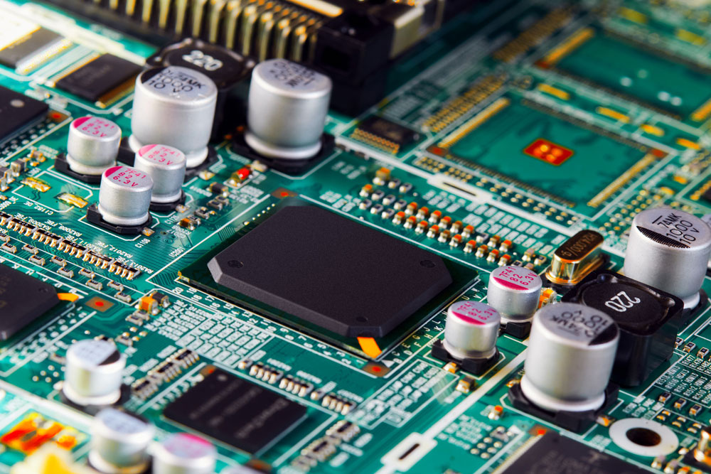
While the main purpose of a PCB is to make electronics work, sometimes the way a board looks can be quite important, too. For some projects, especially those where the inside of a device might be seen, or where a certain brand image is desired, the visual appeal of the board really matters. It is not just about function; it is about how it presents itself. People often care about this quite a bit.
For instance, some boards come in specific colors, like white, or have special covers, like heatsinks, that are meant to look good. This is particularly true for things like computer components, where enthusiasts often want their internal parts to match a certain theme. It is a bit like choosing the right color for a car; it is about personal taste and overall presentation. You can tell that some thought went into it.
So, people do talk about the "look" of a PCB. It is not just a bland piece of green fiberglass anymore. There is a whole aspect of design that goes into making it visually appealing, too. This can be a real consideration for manufacturers and builders alike. They want things to work, yes, but they also want them to look good, more or less.
Board Aesthetics and PCB Slang Meaning in Appearance
When someone mentions a "white PCB" or a "heatsink jacket" as key features, they are talking about the "pcb slang meaning" related to the board's appearance. These are features that are chosen not just for technical reasons, but for how they contribute to the overall visual appeal. It is about making the board look good, or "having good looks," as some might say. This is quite common in the world of custom computer builds.
For example, a white PCB with a matching heatsink might be chosen specifically for someone building a "pure white" computer system. It is a deliberate choice to make the internal components match a certain visual theme. This goes beyond just making the circuit work; it is about creating a cohesive and pleasing visual experience. It is, in a way, about personal style.
So, when you hear people talking about the "aesthetics" of a board, or its "looks," they are referring to these kinds of visual considerations. It is a part of the design process that caters to personal preference and branding. It is a small but important detail for many people who put these systems together. You know, it is about the whole package.
Why Do We Try Out Boards First?
Before a new electronic device goes into mass production, there is a very important step where you make a small number of boards to test everything out. This is a crucial phase because it lets you catch any problems or make any needed adjustments before you commit to making thousands or millions of them. It is a pretty smart way to avoid costly mistakes.
This process is like a trial run. You have designed your circuit, you have drawn up the plans for the PCB, and now you need to see if it actually works in the real world. You send your design to a factory, and they produce a small batch just for you to check. It is a necessary step to ensure quality and functionality. You really want to get it right before going big.
So, when people talk about this stage, they are referring to the initial production run, meant for evaluation. It is about making sure that what looks good on paper also performs well physically. This step saves a lot of headaches down the line, believe me. It is a fundamental part of bringing any new electronic product to life, more or less.
Prototyping and PCB Slang Meaning for Testing
The term "PCB prototyping" or "打样" (dǎyàng in Chinese, meaning "proofing" or "sampling") is a common piece of "pcb slang meaning" that refers to this initial trial production. It is the process where an electronics engineer, after finishing their circuit design and PCB layout, sends it to a factory for a small batch run. It is essentially a test drive for the board.
This "prototyping" phase is incredibly important because it allows engineers to verify their designs in a physical form. They can check for things like signal integrity, power delivery, and whether all the components fit correctly. It is a chance to find and fix any issues before the expensive mass production begins. You want to iron out all the kinks, so to speak.
So, when someone talks about "prototyping a PCB," they are talking about this critical testing stage. It is about making a few samples to make sure everything is perfect before committing to a large order. It is a very practical and necessary part of the development process. This phrase is well-known among anyone involved in bringing new electronic products to market.
What Materials Are These Boards Made From?
PCBs are not just made of any old material; they are usually crafted from something quite specific that has particular properties. The material needs to be strong, stable, and good at insulating electricity, while also allowing copper traces to be formed on its surface. There is a common choice that nearly everyone in the industry uses, and it is a pretty reliable option.
This material is designed to withstand the heat generated by electronic components and to keep the electrical signals separated from each other. It is a composite material, meaning it is made from a mix of different things, put together to create something with the right characteristics. You know, it is engineered for a specific job.
So, when people talk about the "stuff" a PCB is made of, they are often referring to this standard material. It is a very important part of the board's performance and durability. The choice of material is not arbitrary; it is based on years of experience and testing. It has to be just right for the job, in a way.
The Common Stuff and PCB Slang Meaning for Materials
The material most commonly used for PCBs is called "FR-4." This is a bit of "pcb slang meaning" that refers to "Glass Fiber Reinforced Epoxy." It is a high-performance composite material, which basically means it is a mix of glass fiber and epoxy resin. It is the go-to choice for many reasons, including its strength and electrical insulation properties. It is a very familiar term for anyone working with these boards.
Think of it like this: the glass fibers give it strength and stability, kind of like rebar in concrete, while the epoxy resin holds it all together and provides the necessary insulation. This combination makes FR-4 a very reliable base for all the delicate electronic circuits. It is able to handle a lot of different conditions, which is pretty useful.
So, when someone says "FR-4," they are talking about the basic building block of most PCBs. It is the standard material that forms the bulk of the board. This term is widely understood and used among people who design, manufacture, or even just work with electronic devices. It is the typical stuff you see, you know.
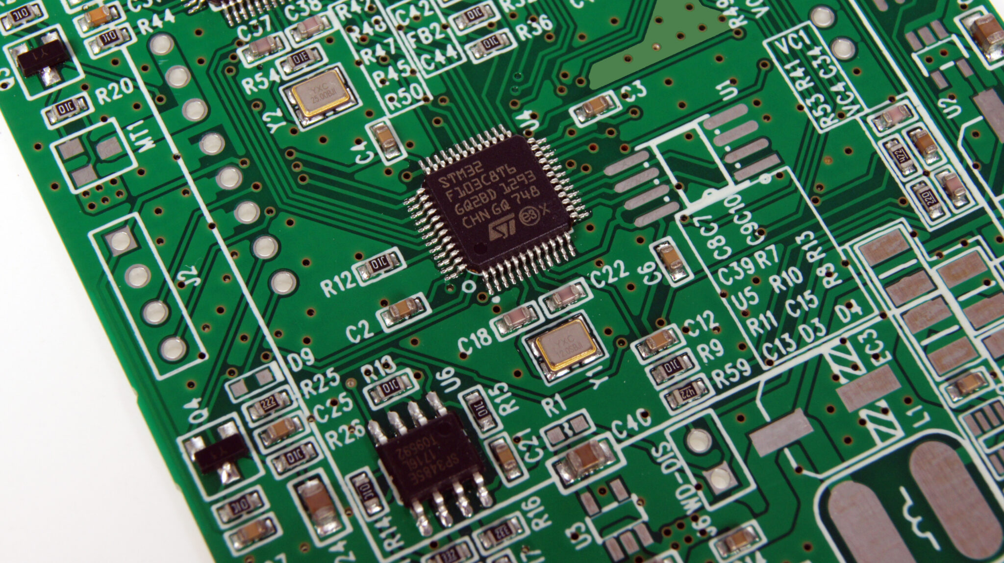
How Do Software Tools Fit into All This?
Designing a PCB today is not done by hand with a pencil and paper, at least not usually. It is almost entirely done using specialized computer programs. These programs help engineers draw the circuits, arrange the components, and lay out all the tiny copper lines on the board. They are pretty essential for modern design work, really.
There are several different software tools available, each with its own strengths and fan base. Some are very popular in certain parts of the world, or for particular types of projects. Learning to use one of these programs is a big part of becoming a PCB designer. It is where all the magic happens, so to speak.
So, when people talk about "drawing PCB diagrams" or "doing layout," they are often referring to using these software packages. They are the digital workbench where the board takes shape before it is ever physically made. These tools are what allow for complex designs to be created efficiently and accurately. They are, in a way, the modern designer's best friend.
Design Helpers and PCB Slang Meaning for Software
When people list names like "Cadence Allegro," "Mentor PADS," "Altium Designer," or "Zuken," they are giving you some "pcb slang meaning" related to the software tools used for PCB design. These are the big names in the world of electronic design automation, or EDA, as it is sometimes called. Each one has its own community of users and a particular way of doing things.
Altium Designer, for instance, is quite popular in many places, while Zuken tools might be more common in Japan. These programs allow designers to create both the schematic, which is the logical diagram of the circuit, and the layout, which is the physical arrangement of components and traces on the board. They are the digital canvases for circuit creation, apparently.
There are also newer options, like JiaLiChuang EDA (JLCPCB EDA), which is a cloud-based tool. This means you can use it right in your web browser, without having to install anything special on your computer. This kind of flexibility is a big deal for many people, as it makes getting started much easier. So, when people talk about "EDA tools" or specific software names, they are referring to these essential design helpers.
What Is the Difference Between PCB and PCBA?
Sometimes, people use the terms PCB and PCBA interchangeably, but there is actually a very important difference between them. Knowing this distinction is key to understanding conversations in the electronics world. It is a bit like knowing the difference between a house frame and a finished house; one is a component, the other is a complete assembly. You know, they are related but distinct.
One refers to just the bare board, the blank canvas, while the other refers to that board with all the electronic parts already attached and soldered on. This distinction is quite fundamental to how things are discussed in manufacturing and design. It is a common point of confusion for newcomers, but once you get it, it is pretty clear.
So, when people are talking about these two terms, they are often emphasizing whether they mean just the foundational board or the board with all its components ready to go. It is about moving from a basic piece to a functional unit. This difference is important for ordering, manufacturing, and even just talking about a product's stage of completion.
Bare Board Versus Finished Product and PCB Slang Meaning Distinctions
The "pcb slang meaning" around PCB and PCBA highlights a critical difference. A "PCB" refers to the bare printed circuit board itself, without any components attached. It is just the fiberglass material with the copper traces etched onto it, ready for parts to
- Magic Left In Miami
- Shannon Sharpe Standing Meme
- Its My Birthday Cash App Me
- Real Diamond Meme
- Romero Y Cebolla Para Que Sirve

Mastering the Art of PCB Design Basics | Sierra Circuits
4 Layer PCB: What You Need to Know
PCB inner layer design - Kingford
